Einleitung
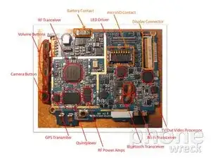
Overview of the Samsung Omnia hardware with circuit diagrams and labeled chips.
Werkzeuge
-
-
The Samsung Omnia is not a “new” device – we had one lying around and all the hype surrounding the fresh Omnia HD had us thinking we might as well break it open to see what makes it hum. The verdict? You’ll have to read on. Simply said however, this device was built for function.
-
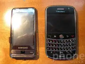
At a time when everybody and their brother/sister seems to be creating an iPhone clone, the Samsung Omnia came out as a fully featured device to meet the requirements and fill the voids that exist in Apples highly acclaimed platform. Man, is this thing packed with features… Let’s see how it stacks up from a design perspective.
-
-
-
The Samsung Omnia is a well built device but it’s no Xperia. Unlike most of the BlackBerry devices we’ve seen the chrome feature around frame of the device is actually metal – not painted plastic that scuffs and scrapes with everyday use.
-
The battery cover and trim pieces that make up the surroundings fit within small tolerances, and there is very little give or “flexible” feeling as you use the device.
-
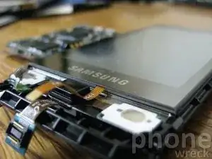
The screen is resistive but doesn’t feel loose like some of the other devices we’ve seen with the same technology.
-
-
-
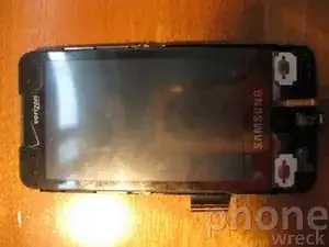
Unfortunately the TouchWiz UI didn’t really tickle our fancy. The 3.2”, 240×400 screen simply isn’t big enough for all of the necessary widgets and you’ll often find yourself accidently moving the icons around the screen. Moreover, the screen seems fairly small for the overall size of the device. From an aesthetics perspective, it’s a little too tall and narrow. We found ourselves often wishing for a little bit more real-estate during typing related activities.
-
-
-
What’s with the proprietary headphone/USB/Tv-out jack? It’s really cool that all of these functions are provided via a single jack, but sometimes you don’t have the specific Samsung cable handy. It’s also annoying to plug your 2.5mm headphones into an included adapter. 2.5mm? ??!!! This is like the BlackBerry of 2002!
-
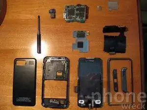
This device is well built. As such, it was a little bit tricky to take apart. Thankfully, all shielding was clip in and the device’s brains were easily revealed. Muahahahaha.
-
The block diagram can be found here.
-
-
-
This device is well built. As such, it was a little bit tricky to take apart. Thankfully, all shielding was clip in and the device’s brains were easily revealed. Muahahahaha.
-
-
-
The primary IC diagram can be found here.
-
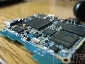
Notably, this device runs on the Qualcomm 6800A and Marvell PXA312. These devices are connected via a Cypress Dual-Port bridge and have separate Power Management Devices. Note that this PCB is impressively packed and impressively small! Another thing to point out is the presence of an SMSC USB PHY. We’ve seen these devices on a variety phones we’ve ripped apart.
-
Bluetooth goes to CSR and Wi-Fi to Marvell. The GPS win goes to Avago. Note the massive quintplexer!
-
-
-
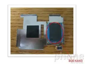
The one thing we knew the phone had but couldn’t find was the 8GB internal memory. Where could it be? We eventually found it hiding underneath the shield covering the processor side of the PCB - very sneaky!
-
